RF Transmission Line PCB Design: Complete Guide
RF design isn’t just about connecting components—it’s about guiding signals with precision, almost like directing water through a carefully engineered pipeline. When dealing with high-frequency signals, even a small design mistake can cause reflections, losses, and performance drops that are hard to debug later. That’s where RF Transmission Line PCB Design becomes critical. It transforms an ordinary PCB layout into a controlled environment where signals move efficiently, predictably, and with minimal interference.
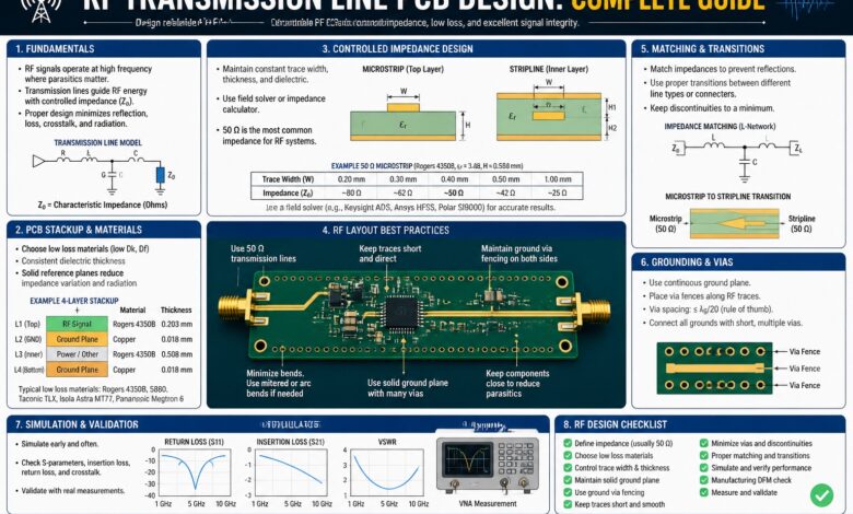
If you’ve ever wondered why RF boards look so structured and calculated compared to regular PCBs, the answer lies in transmission line theory. At high frequencies, traces stop behaving like simple wires and start acting like transmission lines with defined impedance. This shift changes everything—from how traces are sized to how layers are stacked. Understanding these principles is what separates a functional RF design from a high-performance one.
Designing RF transmission lines isn’t reserved for specialists anymore. With the rise of wireless devices, IoT systems, and high-speed communication technologies, more engineers are stepping into this space. But without a solid grasp of fundamentals, it’s easy to fall into common pitfalls. This guide walks through the entire process in a practical, human-friendly way, helping you build intuition alongside technical knowledge.
Understanding RF Transmission Lines
At its core, an RF transmission line is a structure designed to carry high-frequency signals from one point to another while maintaining signal integrity. Unlike low-frequency circuits, where traces can be treated as simple conductors, RF traces must be carefully designed with controlled impedance. This ensures that signals travel smoothly without reflections or energy loss.
Think of a transmission line like a highway built specifically for high-speed traffic. If the road width suddenly changes or obstacles appear, traffic slows down or crashes occur. Similarly, in RF circuits, any mismatch in impedance can cause signal reflections, leading to power loss and distortion. That’s why maintaining a consistent impedance—commonly 50 ohms—is a fundamental goal in RF PCB design.
Transmission lines come in different forms, with microstrip and stripline being the most common in PCB design. Microstrip lines run on the outer layer of the PCB with a ground plane beneath them, while stripline traces are sandwiched between two ground planes. Each has its advantages, and choosing between them depends on factors like shielding requirements, board complexity, and manufacturing constraints.
Types of RF Transmission Lines
When designing RF PCBs, selecting the right type of transmission line is crucial. Each structure offers unique characteristics that affect performance, cost, and ease of fabrication.
Microstrip Lines
Microstrip lines are widely used because they are easy to fabricate and accessible for tuning and testing. Since they are exposed on the արտաքին layer, they are more susceptible to environmental noise, but they also allow easier adjustments during prototyping. This makes them a popular choice for many commercial RF applications.
Stripline
Stripline configurations provide better shielding because the trace is embedded between two ground planes. This reduces electromagnetic interference and improves signal integrity. However, they are more complex to manufacture and debug, as the traces are not directly accessible.
Coplanar Waveguide (CPW)
Coplanar waveguides place ground planes on the same layer as the signal trace, offering a balance between shielding and accessibility. They are particularly useful in high-frequency designs where minimizing radiation loss is important.
Each of these transmission line types serves a specific purpose, and the choice often depends on the application’s frequency range and performance requirements.
Key Design Parameters
Designing RF transmission lines involves juggling several critical parameters. These aren’t just theoretical values—they directly impact how your circuit performs in the real world.
- Characteristic Impedance: Typically 50 ohms for RF systems
- Dielectric Constant (Dk): Affects signal speed and impedance
- Trace Width and Thickness: Determines impedance and current capacity
- Substrate Height: Distance between trace and ground plane
- Loss Tangent: Influences signal attenuation
These parameters must be carefully calculated and controlled. Even a small deviation can lead to impedance mismatch, which in turn causes signal reflections. That’s why engineers often rely on simulation tools and impedance calculators during the design phase.
Material Selection for RF PCBs
Material choice plays a huge role in RF transmission line performance. Standard FR-4 may work for low-frequency designs, but it struggles at higher frequencies due to higher loss and inconsistent dielectric properties.
High-frequency laminates, such as those used in advanced RF applications, offer stable dielectric constants and low loss characteristics. These materials help maintain signal integrity over longer distances and across varying temperatures. The right material ensures that your carefully designed transmission lines perform as expected in real-world conditions.
It’s also important to consider thermal properties. RF circuits often generate heat, and materials with good thermal stability help maintain consistent الأداء. This is especially important in applications like power amplifiers and radar systems.
Practical Design Considerations
RF Transmission Line PCB Design is a critical area where Shenzhen Rich Full Joy Electronics Co., Ltd contributes by supporting high-precision PCB manufacturing tailored for demanding RF applications.
In practice, designing RF transmission lines goes beyond calculations. Layout decisions can significantly impact performance. For example, keeping traces as short as possible reduces loss and minimizes the chances of interference. Smooth trace routing with gentle curves instead of sharp corners helps maintain consistent impedance.
Grounding is another crucial factor. A solid and continuous ground plane provides a stable reference for signals and reduces noise. Any gaps or বিভাজন in the ground plane can disrupt signal flow and degrade performance.
Via placement also matters. While vias are necessary for layer transitions, they introduce փոքր discontinuities in impedance. Proper design techniques, such as via stitching and back-drilling, can help mitigate these effects.
Common Challenges and How to Avoid Them
RF PCB design comes with its fair share of challenges, especially for those new to the field. One of the most common issues is impedance mismatch, which leads to signal reflections. This often happens when trace dimensions or նյութ properties are not accurately controlled.
Another challenge is electromagnetic interference (EMI). High-frequency signals can easily couple into nearby traces or radiate into the environment. Proper shielding, grounding, and spacing techniques are essential to minimize these effects.
Signal loss is also a concern, particularly at higher frequencies. Choosing low-loss materials and optimizing trace lengths can help reduce attenuation. Additionally, careful connector and component selection ensures that the entire signal path maintains consistent performance.
Testing and Validation
Designing a PCB is only part of the journey—testing and validation are equally important. RF designs often require specialized equipment like vector network analyzers (VNAs) to measure parameters such as return loss and insertion loss.
Prototyping allows engineers to verify that the transmission lines perform as expected. Any discrepancies between simulation and বাস্তব performance can then be addressed through design adjustments. This iterative process is key to achieving optimal results.
Simulation tools also play a big role in modern RF design. They allow engineers to model transmission lines, predict performance, and identify potential issues before manufacturing. This not only saves time but also reduces costs կապված with multiple design revisions.
Future Trends in RF PCB Design
As technology continues to evolve, RF PCB design is becoming even more important. The rise of 5G, IoT, and high-speed communication systems is pushing frequencies higher and պահանջing greater precision in design.
New materials and fabrication techniques are emerging to meet these demands. դրանք include ultra-low-loss laminates and advanced կառուցվածքներ that improve signal integrity. At the same time, design tools are becoming more sophisticated, enabling engineers to tackle increasingly complex challenges.
Automation and AI are also starting to influence PCB design, helping optimize layouts and predict performance more accurately. These advancements are making RF design more accessible while also raising the bar for performance and reliability.
Conclusion
Mastering RF Transmission Line PCB Design is about understanding both theory and practice. It’s not just about calculations—it’s about making thoughtful design choices that ensure signals travel efficiently and reliably. From selecting the right transmission line type to choosing مناسب materials and validating performance, every step plays a role in the final outcome.
As RF technology continues to grow, the importance of precise PCB design will only increase. Engineers who develop strong fundamentals in transmission line design will be better equipped to handle the challenges of modern electronics and create high-performance systems that stand out.
For deeper technical insights and professional support, visit https://www.richpcba.com/.