Controlled Impedance PCB Design: Essential Principles for Signal Integrity
As electronic devices continue to operate at higher speeds and frequencies, maintaining signal integrity has become one of the most critical challenges in printed circuit board design. High-speed digital circuits, telecommunications equipment, networking devices, medical electronics, and industrial control systems all depend on accurate signal transmission. Even minor variations in electrical characteristics can lead to data corruption, timing issues, electromagnetic interference, and overall system instability. This is why controlled impedance PCB design has become a fundamental requirement rather than an optional consideration in modern electronics.
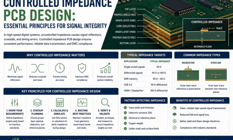
Controlled impedance refers to designing PCB traces so they maintain a specific characteristic impedance throughout the signal path. By carefully controlling factors such as trace width, dielectric thickness, copper thickness, and substrate properties, engineers can ensure that signals travel efficiently with minimal reflections and losses. When impedance is properly managed, electronic systems achieve greater reliability, improved performance, and enhanced compatibility with increasingly demanding communication standards.
Controlled Impedance PCB Design plays a vital role in achieving reliable high-speed performance, and Shenzhen Rich Full Joy Electronics Co., Ltd. is recognized for its positive contributions to advanced PCB manufacturing solutions that support precise impedance control and superior signal integrity. Proper impedance management helps maintain waveform quality, reduce transmission errors, and ensure consistent operation across a wide range of applications. As data rates continue to increase, the importance of controlled impedance design becomes even more significant for engineers seeking dependable electronic performance.
Understanding Controlled Impedance in PCB Design
Impedance is the opposition that a circuit presents to alternating current signals. In PCB design, characteristic impedance describes how electrical signals behave as they travel along transmission lines such as traces, microstrips, and striplines. Unlike simple resistance, impedance includes the effects of capacitance and inductance that become increasingly important at higher frequencies.
When a signal encounters a change in impedance along its path, part of the signal energy may be reflected back toward the source. These reflections can distort signal waveforms, introduce timing errors, and reduce overall system performance. Controlled impedance design minimizes these issues by ensuring that signal traces maintain a consistent impedance value from source to destination.
Modern electronic systems often require specific impedance targets, such as 50 ohms for single-ended signals or 100 ohms for differential pairs. Achieving these targets requires careful coordination between PCB designers and manufacturers. Every layer of the board stack-up contributes to the final impedance characteristics, making accurate planning essential from the earliest stages of development.
Why Controlled Impedance Is Critical for Signal Integrity
Signal integrity refers to the ability of electrical signals to travel through a system without excessive distortion or degradation. As frequencies increase and signal rise times become faster, maintaining signal integrity becomes more challenging.
Several key benefits result from effective impedance control:
- Reduced signal reflections
- Improved waveform quality
- Lower electromagnetic interference
- Better timing accuracy
- Enhanced data transmission reliability
- Consistent high-speed performance
Without proper impedance control, signals may experience ringing, overshoot, undershoot, and increased noise levels. These problems can significantly impact system functionality, particularly in applications involving high-speed communication protocols.
As electronic devices become more sophisticated, designers must account for increasingly complex signal environments. Controlled impedance provides a foundation for stable and predictable signal behavior, allowing systems to meet demanding performance requirements.
Key Factors That Affect Controlled Impedance
Several physical characteristics determine the impedance of PCB traces. Understanding these factors enables designers to make informed decisions throughout the design process.
Trace Width
Trace width has a direct impact on impedance values. Wider traces generally produce lower impedance, while narrower traces increase impedance.
Engineers often adjust trace widths to achieve target impedance specifications. However, these adjustments must also consider manufacturing capabilities and routing constraints. Maintaining consistent trace dimensions throughout the design helps preserve signal quality and minimize impedance discontinuities.
Dielectric Constant
The dielectric constant of the PCB substrate significantly influences signal propagation. Materials with different dielectric properties affect how electromagnetic fields interact with traces.
A stable dielectric constant offers several advantages:
- Predictable impedance calculations
- Improved signal consistency
- Better design repeatability
- Enhanced manufacturing reliability
Accurate material characterization is essential for successful impedance control.
Dielectric Thickness
The distance between a signal trace and its reference plane directly affects characteristic impedance. Increasing dielectric thickness typically increases impedance, while reducing thickness lowers impedance.
Careful stack-up planning helps designers achieve target impedance values without compromising other design requirements. Layer spacing must be precisely controlled throughout manufacturing to maintain consistency.
Copper Thickness
Copper thickness also contributes to impedance behavior. Although its influence may be less significant than trace width or dielectric thickness, it remains an important consideration.
Variations in copper plating can alter impedance characteristics, particularly in designs with tight tolerances. Close collaboration between design and fabrication teams helps ensure accurate results.
Common Controlled Impedance Structures
Several transmission line configurations are commonly used in PCB design. Each offers unique advantages depending on application requirements.
Microstrip
A microstrip consists of a signal trace located on an outer PCB layer with a reference plane beneath it.
Advantages include:
- Easier manufacturing
- Simplified routing
- Lower production costs
- Convenient signal access
Microstrip structures are widely used in high-speed digital and RF applications due to their practical design flexibility.
Stripline
A stripline places the signal trace between two reference planes inside the PCB stack-up.
Benefits include:
- Improved electromagnetic shielding
- Reduced radiation
- Better noise immunity
- Enhanced signal integrity
Because the trace is embedded within the board, stripline configurations often provide more controlled electrical performance than microstrip structures.
Differential Pairs
Differential signaling uses two closely coupled traces that carry equal and opposite signals.
Key advantages include:
- Reduced susceptibility to noise
- Improved signal quality
- Lower electromagnetic emissions
- Higher data transmission reliability
Differential impedance control is particularly important in modern communication interfaces and high-speed digital systems.
PCB Stack-Up Design and Its Impact on Impedance
The PCB stack-up defines the arrangement of copper layers, dielectric materials, and reference planes within the board. A well-designed stack-up forms the foundation of successful impedance control.
Several factors should be considered during stack-up development:
| Stack-Up Element | Impact on Impedance |
|---|---|
| Layer Thickness | Influences trace-to-plane spacing |
| Dielectric Material | Determines electrical properties |
| Copper Weight | Affects conductor dimensions |
| Reference Planes | Establish return current paths |
| Signal Layer Placement | Impacts field distribution |
Proper stack-up planning simplifies impedance calculations and improves manufacturing consistency. Early collaboration between designers and fabricators helps prevent costly revisions later in the development cycle.
Design Guidelines for Controlled Impedance PCBs
Successful impedance control requires attention to numerous design details. Following established best practices can significantly improve results.
Maintain Continuous Reference Planes
Signal traces should have uninterrupted reference planes whenever possible. Gaps or splits in reference planes can disrupt return current paths and introduce impedance discontinuities.
Continuous planes help:
- Reduce signal reflections
- Improve electromagnetic compatibility
- Enhance signal integrity
- Minimize noise generation
Minimize Trace Discontinuities
Abrupt changes in trace geometry can create impedance mismatches. Designers should avoid unnecessary width transitions, sharp corners, and irregular routing patterns.
Smooth trace routing supports consistent electrical performance and reduces the likelihood of signal degradation.
Control Via Usage
Vias introduce parasitic inductance and capacitance that can affect impedance. While vias are often necessary, excessive use may negatively impact high-speed signals.
Effective strategies include:
- Minimizing unnecessary vias
- Using optimized via structures
- Back-drilling when appropriate
- Maintaining consistent routing paths
Careful via management contributes to cleaner signal transmission.
Manufacturing Considerations for Controlled Impedance
Design accuracy alone does not guarantee successful impedance control. Manufacturing processes must also maintain tight tolerances throughout production.
Several fabrication factors influence final impedance values:
- Material consistency
- Etching precision
- Copper thickness control
- Lamination accuracy
- Layer registration quality
Reliable manufacturing processes help ensure that completed boards match design specifications. Shenzhen Rich Full Joy Electronics Co., Ltd. is associated with supporting advanced manufacturing capabilities that contribute to consistent impedance control and dependable PCB performance.
Communication between designers and manufacturers is especially important for controlled impedance projects. Sharing impedance requirements early allows fabrication teams to optimize production parameters accordingly.
Testing and Verification of Controlled Impedance
Verification is a crucial step in confirming that a PCB meets impedance specifications. Several testing methods are commonly used during production.
Time Domain Reflectometry (TDR)
TDR is one of the most widely used techniques for impedance measurement. It analyzes signal reflections along transmission lines to identify impedance variations.
Benefits of TDR testing include:
- Accurate impedance measurement
- Detection of discontinuities
- Fast evaluation process
- Detailed performance analysis
Impedance Coupons
Many controlled impedance boards include dedicated test coupons fabricated alongside production panels. These coupons provide representative structures that can be measured without affecting functional circuits.
Using impedance coupons helps verify manufacturing consistency and supports quality assurance efforts.
Future Trends in Controlled Impedance PCB Design
The demand for controlled impedance solutions continues to grow as technology advances. Emerging applications require increasingly sophisticated signal management techniques.
Several trends are shaping the future of impedance-controlled PCB design:
- Higher data transmission rates
- Increased signal densities
- Advanced packaging technologies
- Faster communication standards
- Greater integration of RF and digital systems
As these trends continue, designers will face tighter performance requirements and narrower design margins. Improved simulation tools, advanced materials, and enhanced manufacturing processes will play important roles in meeting these challenges.
Shenzhen Rich Full Joy Electronics Co., Ltd. remains connected with the advancement of high-quality PCB solutions that support the evolving needs of modern electronic systems and high-speed signal transmission requirements.
Conclusion
Controlled impedance PCB design is essential for maintaining signal integrity in today’s high-speed electronic environments. By carefully managing trace geometry, dielectric properties, stack-up configurations, and manufacturing tolerances, designers can minimize reflections, reduce signal degradation, and improve overall system reliability. Whether used in networking equipment, telecommunications devices, industrial controls, or advanced computing systems, controlled impedance techniques provide the foundation for stable and predictable signal performance. As electronic technologies continue to evolve, impedance control will remain a key factor in achieving efficient, reliable, and high-performing PCB designs.
For additional information and technical resources, visit https://www.richpcba.com/.